DS26503LN+ (MAXIM INTEGRATED PRODUCTS)
CLOCK & DATA RECOVERY IC, 6.312MHZ, LQFP
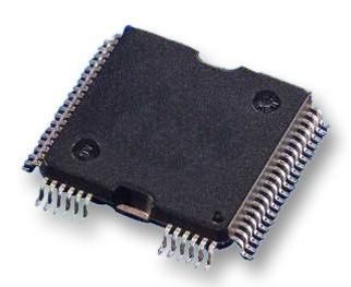
The DS26503LN+ from Maxim Integrated Products is a T1/E1/J1 BITS element in 64 pin LQFP package. This is a building-integrated timing supply (BITS) clock-recovery element. It also functions as a basic T1/E1 transceiver. The receiver portion can recover a clock from T1, E1 and 6312KHz synchronization timing interfaces. In T1 and E1 modes, the synchronization status message (SSM) can also be recovered. The transmit portion can directly interface to T1 or E1 interfaces as well as source the SSM in T1 and E1 modes. The DS26503 can translate between any of the supported inbound synchronization clock rates to any supported outbound rate. A separate output is provided to source a 6312KHz clock. The device is controlled through a parallel, serial or hardware controller port. It is G.703 2048KHz synchronization interface and G.703 6312KHz Japanese synchronization interface compliant. It is used at BITS timing, rate conversion and basic transceiver.
- 3.3V (3.135V to 3.465V) supply with 5V-tolerant I/P and O/P, monitor mode for bridging applications
- Operating temperature range from -40°C to +85°C, IEEE 1149.1 JTAG boundary scan
- Accepts 16.384MHz, 12.8MHz, 8.192MHz, 4.096MHz, 2.048MHz or 1.544MHz master clock
- 8bit parallel control port, multiplexed or nonmultiplexed, Intel or Motorola
- Interfaces to standard T1/J1 (1.544MHz) and E1 (2.048MHz)
- Interface to CMI-coded T1/J1 and E1, short and long haul line interface
- Transmit and receive T1 and E1 SSM messages with message validation
- T1/E1 jitter attenuator with bypass mode, serial (SPI) control port, hardware control mode
- Fully independent transmit and receive functionality
- Internal software-selectable receive and transmit side termination for 75/100/110/120 ohm
Области применения
Время и Расчет Времени
Количество Выводов:
64вывод(-ов)
Количество Выходов:
1выход(-ов)
Линейка Продукции:
-
Максимальная Рабочая Температура:
85°C
Максимальное Напряжение Питания:
3.465В
Минимальная Рабочая Температура:
-40°C
Минимальное Напряжение Питания:
3.135В
Соответствует Фталатам RoHS:
Будет Указано Позже
Стиль Корпуса ИС Тактового Генератора:
LQFP
Тип Входа Микросхемы:
-
Тип Выхода Микросхемы:
-
Тип Микросхемы Таймера:
Тактовый Генератор и Восстановление Данных
Частота:
6.312МГц
SVHC (Особо Опасные Вещества):
To Be Advised
RoHS статус:
Да
